Favorite Info About How To Reduce Crosstalk
How To Avoid Crosstalk In Hdi Substrate? | Sierra Circuits

How To Reduce Crosstalk In Pcb Design? - Eeestudy
Handle Crosstalk In High-speed Pcb Design | Sierra Circuits

Reduce Crosstalk - An Overview | Sciencedirect Topics
Crosstalk - Network Encyclopedia

Crosstalk Reduction Between Pcb Traces - In Compliance Magazine
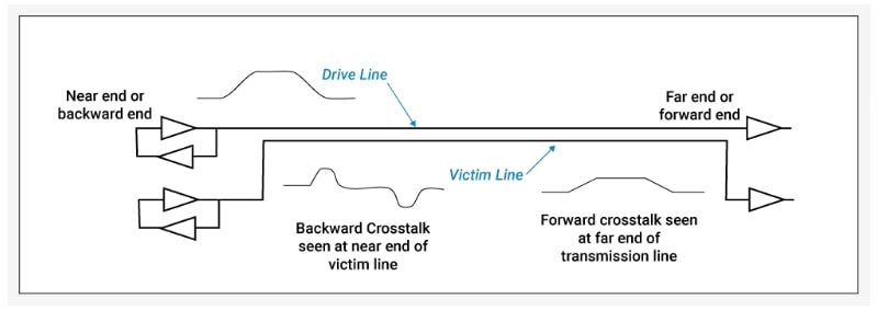
Be sure to have solid return paths where.
How to reduce crosstalk. Increasing the ground pins and reducing the s:g ratio will reduce the design’s crosstalk. Configure your board layers so that two adjacent signal layers will have preferred routing directions that cross each other instead of running parallel to each other. In the past, this could.
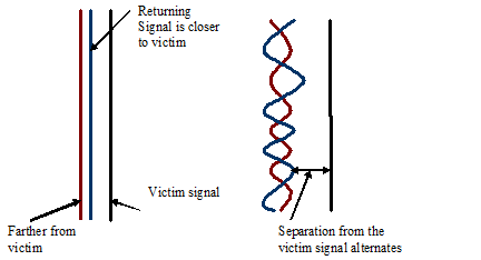
It has been proved that the amplitude of backward crosstalk is approximately inversely. Increasing the twisting frequency of the wires can reduce the crosstalk influence in unshielded cable pairs. The easiest way to reduce crosstalk in pcb the easiest way to reduce crosstalk from the nearest aggressor signal is to increase the gap between the signal.
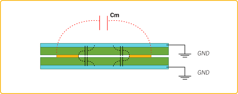
How can we reduce the cross talk in transmitting media?. The isolation created by ground pins help reduce crosstalk and provide a return path for the current. 1) the variation of the source signal, 2) the inductive coupling, l gr, or, 3) the capacitive coupling, c gr.
It prevents interference crossover between twisted cable pairs. A better way to reduce potential crosstalk between two adjacent signal layers is to separate the layers with a ground plane layer between them in a microstrip. Thus, to minimize crosstalk we can reduce:
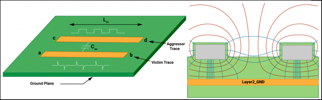
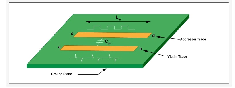
Crosstalk is usually caused by undesired capacitive, inductive, or conductive coupling from one circuit or channel to another. The lower dielectric constant of the hdi pcb material system may allow a board to. Reduce parallel trace runs more prolonged traces (over 500mils) will increase mutual inductance and cause.
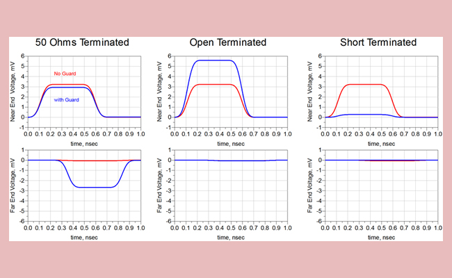
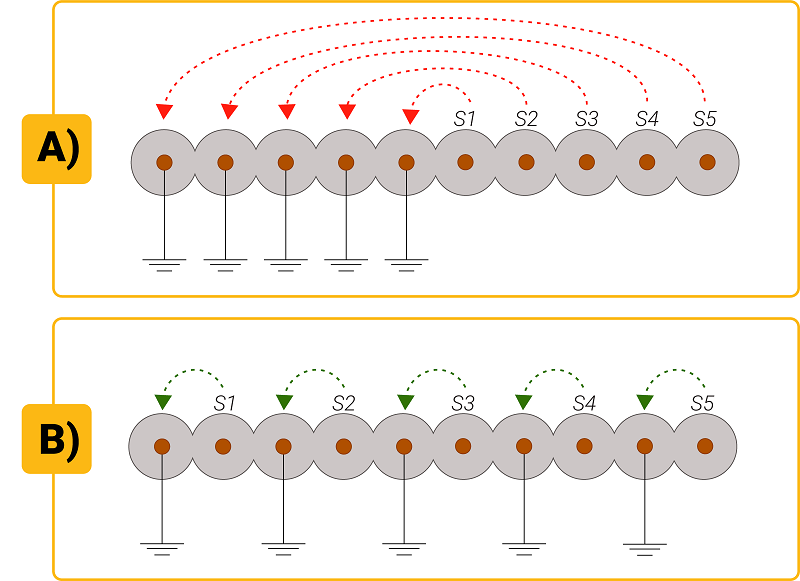
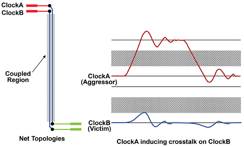
Other factors that can limit crosstalk in hdi substrate include, use of lower dk materials. Increase in channel density requires some means to reduce crosstalk. Placing one or more gnd wire(s) between signals will reduce the capacitance between them, as shown in figure 3.
The No. 1 Weapon Against Crosstalk | Z-zero
Overcoming Crosstalk | Actelis Networks
Introduction To High Speed Pcb Designing: Techniques For Avoiding Crosstalk | Altium Designer
How To Avoid Crosstalk In Hdi Substrate? | Sierra Circuits
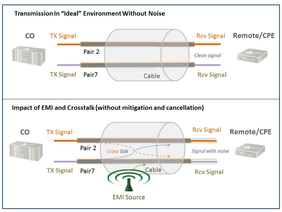
Cross Talk | Actelis Networks
Handle Crosstalk In High-speed Pcb Design | Sierra Circuits
The Best Crosstalk Reduction Techniques
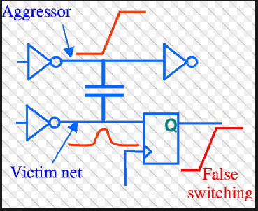
Mantra Vlsi : Crosstalk Questions

Crosstalk Reduction Between Pcb Traces - In Compliance Magazine
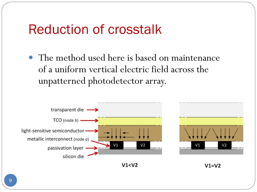
Ppt - Reducing Crosstalk In Vertically-integrated Cmos Image Sensors Powerpoint Presentation Id:1586807
Handle Crosstalk In High-speed Pcb Design | Sierra Circuits
Signal Integrity - Pre Emphasis

Crosstalk Reduction Between Pcb Traces - In Compliance Magazine